Second Generation products - Satellite Radio
A second generation receiver fit on a small board. The articles and press release (click for example) said it all; the small footprint would enable a new category of products and make the devices dashboard mounted. This came true. It is amazing that the devices are only now, in 2010, ending their manufacturing life. This product ran long even by automotive standards.
c.jpg)
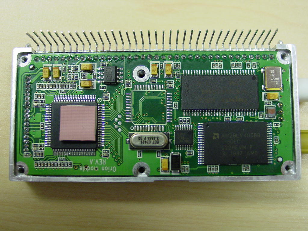
The reverse side of the module contained the baseband and power supply sections . The SDRAM memory and SRAM were also on this board, as was the TCXO.
This page is dedicated to Jalil Fadavi and Stefan Thurnhofer, without whom this Northstar project would not have been possible, and who tragically are no longer with us. Rest in peace.
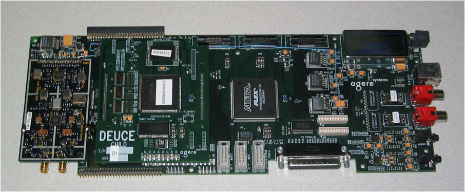
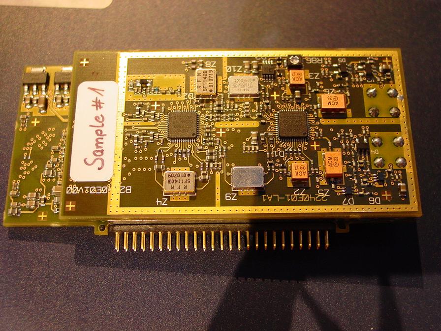
With big efforts, we were able to supply enough parts to the radio manufacturers to enable their development of software, boards, and to assemble our own verification prototypes, The pipeline opened and the products were deployed in the field. Below is a Chip Evaluation Board for second generation. It includes an FPGA and the chip set, with the RF on a separate RF tuner board.
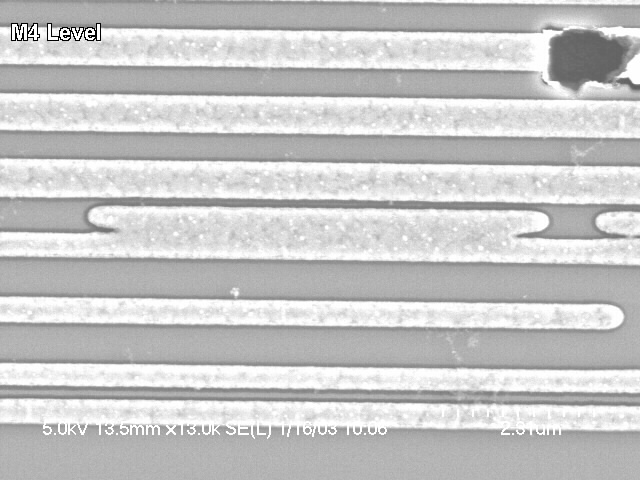
Not quite what the etched metal should look like. Early pains of a new technology went away, eventually.
The 0.14 um process was new, and internally developed. It would be the last process that a $2B company could afford with the increasing demands on economies of scale in the semiconductor industry. The process worked well, but because of the limited resources to get the kinks out,and a few engineering mistakes in the memory area, we found that we threw away one out of ten devices in the beginning. Ours was, I think, the most complex device produced, in terms of the number of transistors. I received really great support from the executives in operations, and we were able to sample the customer.
Shortly before the completion of the first chip set, and in the final stages of the software development, it became clear to all that the solution proposed was not going to fit the market needs.
People were used to
listening to radio on portable devices, which could be battery powered for hours and hours on two penlight batteries. The partitioning of the receiver into the large number of chips in the first generation was too big, consumed too much power, and cost too much. The 12 chip family that made up the receiver (RF, IF, ADC, DDC, COFDM, TDMMRC, CDC, DAP, 3xSRAM, SDRAM) could be reduced to a handful.
The solution to place the complete receiver core functions on a single baseband chip was a bold step. We would rely on an internal process ( 0.14um CMOS) to allow for integration. Power consumption estimates looked reasonable. The RF and IF chips worked well and the risk of touching the RF was not worth the potential business disruption. We attacked the bigger problem of the baseband and ADC, to reduce power and size, and follow the technology trend of the other parts. We also added a few minor bells and whistles.