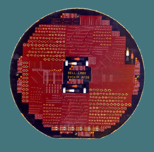
SyChip, Inc
An early product prototype using integrated passives. Discussions with component vendors and a survey of the market showed us quickly that a business model based on passive component sales would not maximize the value of the company.
SyChip was a Lucent spinoff company, receviing funding, over a of time, from Lucent, Pequot, Genesis Park, Global Strategic Investment, the Intel Communications Fund, Markpoint Venture Partners, Masthead, and TechQuest. I joined the effort pre-spinoff during its incubation and business model definition phase in 1999 as VP of Engineering. The company was purchased by Murata in 2006 for approximately 140 Million.
Lucent, at the time, owned a multi-Billion Dollars Microelectronics business with a diversified porfolio. WiFi was emerging, computer connectivity was becoming ubiquitous, and the modem business was still thriving Wireline and Wireless network equipment was in unprecedented demand, magnetic disk storage technology doubled capacity every few years and optical networking semiconductors showed their pre-bubble volume promise.Anticipated demand for seimconductors showed unprecedented growth.
Packaging and testing of Semiconductors, for the most part, was commoditizing, except for niche markets. Continued funding for applied research implemting packaging concepts without the downstream implementations into production lines became of lesser value to the core business.The research performed over the years (I think our CTO alone had something like 100 patents), had tremendous intellectual property value as well as myriad of potential new applications.
Because of this strong foundation, Lucent included Sychip in its spinoff portfolio to leverage the IP and talent. The business model leveraged two core competencies:
While in the incubator, our initial objectives were multifold:
IDaily discussions on the business were animated. A group of three strong minded people with valid opinions would have to converge on a single point of view. From the human dynamics point of view, the startup company is more animated than the large company. Opinions are strong, but always converge. The team has but one goal, to beat the competition, and personal goals are less influential in decisions, since the wrong decisions lead to disaster. As such, a good leadership team always converges after animated debate, and we were no exception. We decided that a pure IP business was not a high return proposition for investors and would become an niche. We also decided that component sales would be a difficult uphill battle considering that the passive component companies ureceived railroad car size material shipments and shipped railroad car sized component shipments. In this ecosystem, every component we build would have to be custom, and efficiency of scale would be difficult to achieve.
Manufacturing custom substrates was also considered as a possibility. At the time, we would compete with Silcon on Insulator (SOI) and LTCC technology, as well as other passive silicon efforts in existence or previously developed, and System in a package offerings from the traditional semiconductor packaging companies. Selling substrates was viable, but did not leverage the full capabilities of the company.
Once we tested the market for the various possible business models, we realized the value of the business had to leverage all the technology under hand, but that sale of a differentiated product would be the only way to leverage the technology to maximize returns. We embarked in several product prototypes, over the year and a half that I was there. A Bluetooth module and a SDRAM memory integration project were quickly followed by an innovative GPS the size of a fingernail. Later, the company built its success on a WiFi SDIO card combination module.
The strategy proved right. Modules were to be sold as commercial assembled and tested components, and software value added, applications support, would provide the end user with valued differntiation. This strategy was applied in the WiFi module manufactured later by Sychip and rebranded by Sandisk and others. Much press is available on this product on the web.

BGA Flip Chip techniques allowed an alternative to stacked die package assemblies and POP packages.
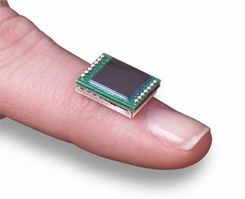
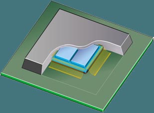
A First for the times, the GPS module included all the components needed for a fully functional unit, into a single 10mmx 11mm module excluding the antenna
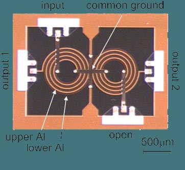
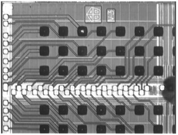
An integrated Passives test wafer comprising of Resistors, Capacitors, and Inductors. These components allowed for a very high density of integration and competed effectively against discrete components for assembly area and volume.
Any wafer can be processed and metallization added to create interconnections on polyimide or other insulating material suitable for semiconductor or packaging processing. The bond pads are rerouted to a matrix of solder balls which can be used to test the IC and also become the assembly mechanism.
This wafer scale apporach is common today, especially in power amplifier and RF devices. By eliminating the wirebond ffound in packages, a much lower inductance can be achieved if the routing is done judiciously. This lower inductance translates into increase in performance or power savings.
.
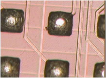
This SDRAM memory was rerouted for eventual flip chip assembly. THe same principles that apply to RF apply to the ability to achieve higher speeds in a device through lower inductance. This also results in power reduction
Memory chips could be flipped and integrated onto a baseband device
Disclaimer: I believe all the information on this site to be either public, or observable by looking at publicly available material, or to have been shared with other parties in the course of business under non disclosure agreements which have long expired at the time of the publication of this website.. Please contact me for any non-compliance with the previous statement. The html code in this site is property of author and under copyright by the author or adobe inc. While all attempts are made to present only factual information, this site contains the opinions of the author and is not in anyway endorsed by his previous employer(s). The purpose of this site is informational; to demonstrate the efforts that can be achieved by a good engineering team, represent an accurate view of the history of such projects, and allow the reader to learn from this history which may parallel other technical and business development. Honest attempts were made to delete corporate logos and trademark if such are not placed on published information such as boards, receivers, or other materials. Please contact me if any violations require remedy.